Cascode GaN power devices use a d-mode HEMT device and offer many advantages in higher-power–conversion applications.The cascode architecture with power gallium nitride devices uses a depletion-mode (d-mode) HEMT device and offers many advantages in higher-power–conversion applications. Improved packaging can help utilize the benefits of GaN to its fullest extent. This article details Nexperia’s development of the copper (Cu)-clip CCPAK package for its cascode power GaN devices, as presented at the December 2023 PowerUP Virtual Expo.
Advantages of cascode GaN architecture
In the cascode architecture, a normally on d-mode HEMT is coupled with a normally off low-voltage silicon MOSFET device, as shown in Figure 1.

The silicon device controls the gate drive, hence offering flexibility in the use of common gate drivers that are used to drive silicon MOSFETs. With the use of a high-threshold–voltage (Vth) MOSFET, the gate drive becomes very robust, allowing for a high overdrive margin and external gate voltages (Vgs) of ±20 V. This is in sharp contrast to the low Vth (< 2 V) typical in enhancement-mode (e-mode) GaN devices, where maximum Vgs is typically limited to 6–7 V, which restricts overdrive. The low Vth also places greater constraints in the gate drive, the gate coupling from drain-switching transitions and added parasitic inductances from the package and board layout to minimize noise and oscillation that could cause a parasitic turn-on.
The use of the d-mode GaN HEMT improves its on-state performance with improved carrier mobility, as well as the off state with a much lower gate leakage from the cascode silicon device. The improved on-state performance translates to higher-current–rated devices. Another key advantage of the cascode arrangement with the d-mode devices is its improved performance at higher temperatures. As shown in Figure 2, e-mode devices (shown under the competitor heading) show a fall in drain current of over 100% from 25°C to 150°C, while the cascode devices show a smaller change at high temperatures.

Silicon carbide MOSFETs, much like silicon MOSFETs, exhibit zero-temperature crossing in their transfer curves. While it is generally advantageous for thermal runaway reasons to operate with the maximum rating on the negative drain-current temperature coefficient part of the curve, the cascode device characteristics allow for the use of devices with less of a derating in the maximum high-temperature power ratings compared with e-mode devices, leading to improved efficiency. The characteristics of the cascode device make it more forgiving in the use of simpler bootstrap gate drivers.
Another key advantage of the d-mode cascode architecture is the much lower third-quadrant voltage drop under reverse conduction, as shown in Figure 3. This arises from the fact that the only significant voltage drop is from the low-voltage silicon MOSFET body diode. The lower voltage drop can increase the flexibility in the deadtime of the circuit (shown as times A and B in Figure 3) and lower deadtime loss for a given deadtime. This loss can be exacerbated for e-mode devices if a negative Vgs is used at turn-off, as is often the case due to the low Vth of the device. The lower deadtime losses can also translate into improved reliability in reverse conduction, compared with degradation from potentially high losses in the e-mode GaN case and body diode degradation in the SiC MOSFET.

Cu-clip packages for GaN
Nexperia has over 20 years of experience in the use of Cu-clip packages for silicon MOSFET devices. This package is called the LFPAK. Over 1.7 billion LFPAK devices were shipped in 2021, Called the LFPAK. Over 1.7 billion LFPAK devices were shipped in 2021, showing the vast acceptance of this package across many applications, including automotive.
Building on this experience, Nexperia is introducing Cu-clip packages for its 650-V GaN power devices. This package is called the CCPAK1212, the numbers designating the 12 × 12-mm size. As shown in Figure 4, both bottom-side– and top-side–cooled CCPAK1212 package offerings are planned. In the case of the top-side–cooled option, the device is flipped and the source-cooling tab is on top. This can offer flexibility in the use of the PCB space and can further improve heat dissipation.

Some of the main advantages of the Cu-clip package compared with other packages are:
● A lower thermal resistance (Rth) and package-added electrical resistance. The large cross-sectional area of Cu improves both electrical and thermal performance compared with traditional wire-bonded packages. This is true even though the package can be much smaller in size in comparison. Soldering the clip directly to the source connection on the die helps prevent areas of high current density seen with bond wires and the resultant hot spots. This also improves reliability at higher power levels. As an example, the maximum junction to mounting base (Rth(j-mb)) of the Nexperia TO-247–packaged 650-V GaN device GAN041-650WSB, rated at a typical on-state resistance RDS(on) of 35 mΩ, Rated at a typical on-state resistance RDS(on) of 35 Mω, is specified at 0.8 K/W. The datasheet of the upcoming 650-V CCPAK1212 top-side -- cooled device GAN039-650NTB, rated at a typical RDS(on) of 33 mΩ, specifies the maximum Rth(j-mb) at 0.5 K/W.
● Lower parasitic inductance. Compared with wire-bonded packages, the parasitic package inductance of the Cu-clip packages can be up to 3× lower. This results in improved switching efficiency and lower electromagnetic interference during switching transitions. This can be especially important in GaN power devices. Their low device capacitances and improved switching figures of merit (FOMs) allow for much faster switching frequencies and transitions. Having low package inductances enables this to be achieved at smaller overshoot levels, providing system-level benefits. The total source-drain inductance in the CCPAK1212 package is only 1.2 nH.In comparison, the same for a competitor’s SiC device in a leadless TOLL package was 2 nH.
● Improved board-level reliability compared with traditional QFN/DFN surface-mounted packages. As shown in Figure 5, the CCPAK has exposed, flexible, gull-winged leads. This allows the CCPAK pins to absorb stress related to thermal expansions and contractions from temperature cycling. In contrast, the fully encapsulated leads in the QFN/DFN packages do not allow any movement in the leads, meaning the solder joint absorbs a lot of the stress, creating risks of joint degradation with temperature cycling. Cracks in the mold also create the risk of early failure in the package.

Cascode GaN performance in CCPAK
The 650-V top-side–cooled CCPAK GaN performance was evaluated under both hard-switching and soft-switching conditions. Figure 6 shows the switching performance of a hard-switching 400-V to 230-V buck converter operating a 100-kHz switching frequency. The excellent Rth allows for high efficiency (> 98%) in this fan-cooled application for power as high as 6 kW. The switching waveform shows a fast rise time of about 7 ns, with an overshoot of less than 20 V.

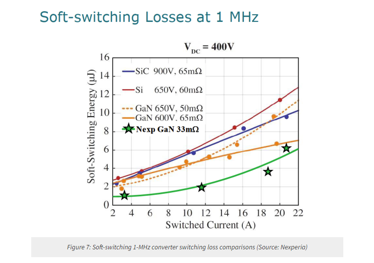
The switching loss comparison of a resonant soft-switching converter at a 400-V DC bus voltage and switching at 1 MHz is shown in Figure 7. The CCPAK GaN device is a lower RDS(on) compared with the rest of the devices shown in Figure 7 and would hence exhibit greater parasitic switching losses for the same FOM. However, the clear FOM advantages of GaN, as well as the cascode and CCPAK package advantages, result in a much lower switching loss for this device compared with the silicon, SiC and e-mode GaN devices.
The cascode architecture and the CCPAK package together serve some of GaN’s inherent benefits to a greater extent. The new 33-mΩ 650-V GaN FETs from Nexperia, offered in a top-side - and bottom-side - cooled CCPAK package, provide many advantages in power-switching applications. GaN HEMTs, with their low reverse-recovery losses, allow for the use of simpler topologies, such as the totem pole for the PFC stage. The much higher switching frequencies with GaN can result in improved power densities and reduced system cost with smaller magnetics.
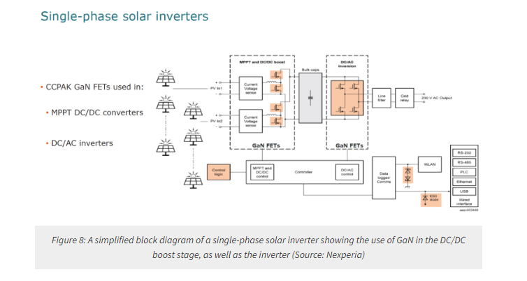
An example application is a single-phase solar inverter. A simplified block diagram of this is shown in Figure 8. Half-bridge GaN devices can be used for the MPPT and DC/DC boost of the incoming PV voltage, while the high-switching GaN devices in the inverter can reduce the size of the line filters and magnetics.
About US
Heisener Electronic is a famous international One Stop Purchasing Service Provider of Electronic Components. Based on the concept of Customer-orientation and Innovation, a good process control system, professional management team, advanced inventory management technology, we can provide one-stop electronic component supporting services that Heisener is the preferred partner for all the enterprises and research institutions.