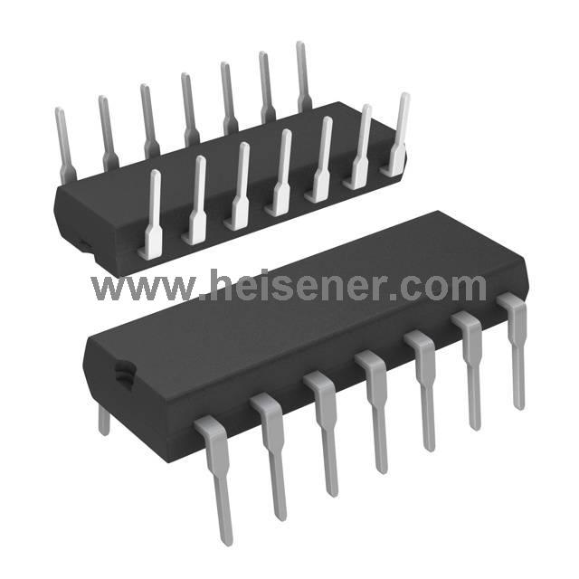
IR2113 Basics
The IR2113 is versatile, high-voltage, high-speed drivers designed to control power MOSFETs and IGBTs with precision and efficiency. They offer independent high- and low-side output channels, making them ideal for demanding power applications. Built with proprietary high-voltage IC (HVIC) and latch-immune CMOS technologies, these drivers are exceptionally robust and resistant to electrical noise, allowing for durable and reliable operation.
These drivers support standard CMOS or LSTTL logic inputs, even down to 3.3V, providing compatibility with modern control systems. Their output stage features a high pulse current buffer, designed to minimize driver cross-conduction and avoid shoot-through currents. Matched propagation delays simplify timing and make the IR2113 well-suited for high-frequency switching applications. Additionally, the floating high-side channel enables control of N-channel MOSFETs or IGBTs at high-side voltages up to 500V or 600V, making these drivers ideal for a wide range of high-voltage applications.
IR2113 Symbol

IR2113 Footprint
IR2113 3D Model

IR2113 Pinout
LO: Low side gate drive output
COM: Low side return
VCC: Low side supply
VB: High side floating supply
VS: High side floating supply return
HO: High side gate drive output
VDD: Logic supply
HIN: Logic input for high side gate driver output (HO), in phase
SD: Logic input for shutdown
LIN: Logic input for low side gate driver output (LO), in phase
VSS: Logic ground
IR2113 Test Circuit


IR2113 Specification
| Specification | Value |
| Number of Drivers | 2 |
| Gate Type | IGBT, N-Channel MOSFET |
| Supply Voltage | 3.3V ~ 20V |
| Logic Voltage - VIL, VIH | 6V, 9.5V |
| Logic Compatibility | 3.3V, CMOS, or LSTTL |
| Peak Output Current | 2A, 2A |
| Propagation Delay | 120 ns |
| High Side Voltage - Max | 600 V |
| Rise / Fall Time (Typ) | 25ns, 17ns |
| Operating Temperature Range | -40°C ~ 150°C |
| Package | 14-DIP |
IR2113 Features
Floating channel designed for bootstrap operation
Fully operational to +500V or +600V
Tolerant to negative transient voltage dV/dt immune
Gate drive supply ranges from 10 to 20V
Undervoltage lockout for both channels
3.3V logic compatible Separate logic supply range from 3.3V to 20V Logic and power ground ±5V offset
CMOS Schmitt - triggered inputs with pull-down
Cycle by cycle edge-triggered shutdown logic
Matched propagation delay for both channels
Outputs in phase with inputs
IR2113 Applications
Induction Heating Systems
Electric Vehicle Charging Stations
Audio Amplifiers
HVAC (Heating, Ventilation, and Air Conditioning) Systems
Appliance Motor Controls
Welding Equipment
High-Voltage Pulse Generators
Grid-Tied Inverters
Electromagnetic Pumps
Medical Imaging Equipment
IR2113 Package
The IR2113 is packaged in a 14-DIP, which is well-suited for high-voltage driver circuit designs. The standard pin pitch for the 14-DIP package is 2.54mm, with overall dimensions of approximately 19.6mm in length, 7.62mm in width, and a thickness of about 3.3mm. The pin height and total package height are designed for easy insertion and soldering onto standard circuit boards.
With the 14-DIP packaging, the IR2113 maintains sufficient spacing between pins to reduce the risk of electrical interference and high-voltage breakdown, making it especially suitable for driving high-voltage MOSFETs and IGBTs.

Guide to Use IR2113
First, connect the power supplies. Connect the VCC pin to the low-side power supply, typically ranging from 10 to 20V, and connect the VDD pin to the logic supply, which supports a range of 3.3V to 20V for standard logic levels. Additionally, connect the VB and VS pins to the high-side floating supply and the high-side floating ground, respectively, so the high-side driver can operate correctly. Ensure that all connections are secure to prevent loose connections.
Next, connect the control inputs. LIN and HIN are the logic inputs for the low-side and high-side, respectively, controlling the LO and HO outputs. Use standard CMOS or LSTTL logic levels to provide input signals, ensuring the voltage levels meet the driver’s requirements. By applying a signal to HIN, you can control HO to output a high level, thus driving the high-side switch. Similarly, by applying a signal to LIN, you can control LO to output a high level, driving the low-side switch. The SD pin is the shutdown input, and when a valid signal is applied, it will simultaneously turn off both high and low-side outputs for protection.
Finally, verify and test the circuit. Before powering on the system, double-check that all connections are correct. To prevent high-frequency noise or electromagnetic interference, you can add appropriate decoupling capacitors. Once the power is applied, gradually adjust the input signals and observe the output behavior to ensure stable operation of the circuit.
FAQs
What is IR2113 used for?
The IR2113 is a high-speed, high-voltage MOSFET and IGBT driver used to drive both the high-side and low-side power transistors in a variety of power electronic circuits. It is particularly useful in applications requiring high voltage and fast switching, such as motor control, power inverters, and other high-power applications.
How does the IR2113 handle high voltage?
The IR2113 features a floating high-side driver that can withstand and operate in high-voltage environments.
What is the typical application for IR2113?
The IR2113 is commonly used in motor drives, power inverters, DC-DC converters, and high-voltage switching circuits.