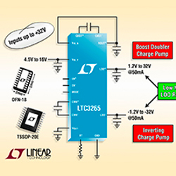
Linear Technology's latest product is LTC3265, which is a new high-voltage, highly integrated, low-noise dual-output power supply that uses a positive input power (VIN_P) and generates up to ± 2 • VIN_P. Low-noise bipolar rail without any noise. Inductor.
The device includes a boost multiplying charge pump, an inverting charge pump, and two low-dropout (LDO) regulators. The boost charge pump has a wide input range of 4.5V to 16V and powers the positive LDO post regulator through its output VOUT +. The inverting charge pump has a larger input range (4.5V to 32V) and can be connected to a boost input or output. The negative LDO post regulator is powered by the output VOUT- of the inverting charge pump. The LTC3265 is particularly suitable for applications that require low-noise bipolar power from high-voltage inputs, such as low noise bias generators for industrial / instrumentation, portable medical equipment, and automotive infotainment systems.
Positive and negative LDO regulators can provide up to 50mA of output current, each output current has an output noise of 100µVRMS, and their output voltage can be independently adjusted from ± 1.2V to ± 32V using external resistor dividers Generates symmetric or asymmetric output power rails. The LTC3265's internal charge pump operates in low quiescent current burst mode (BurstMode®) for maximum efficiency, or in constant frequency mode for lowest noise. In burst mode operation, the LTC3265 consumes only 135µA of quiescent current when the two LDO regulators are at no load. In constant frequency mode, the device operates at a fixed value of 500kHz or a programmed value between 50kHz and 500kHz using an external resistor. Other features of the IC include the small number of external parts and the stability of ceramic capacitors. The
LTC3265 is available in a flat (0.75mm) 3mm x 5mm 18-lead DFN package and a 20-lead TSSOP package, all with back-side thermal pads. Regardless of the package, the E and I operating junction temperature range is -40C to 125C. The H-class operating temperature range is -40C to 150C, while the MP-class operating temperature range is -55C to 150C.